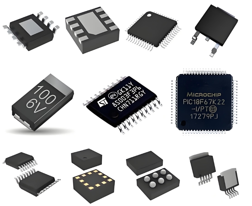
Infineon IRFR3411TRPBF: Key Specifications and Application Circuit Design Considerations
The Infineon IRFR3411TRPBF is a widely adopted N-channel power MOSFET that leverages advanced silicon technology to deliver high efficiency and robustness in a variety of switching applications. This component is particularly valued in power management circuits for its low on-state resistance and fast switching capabilities.
Key Electrical Specifications
A thorough understanding of the device's absolute maximum ratings and electrical characteristics is paramount for reliable circuit design.
Drain-Source Voltage (Vds): The device is rated for a maximum of 55V, making it suitable for a broad range of low-voltage applications, including 12V, 24V, and 48V systems.
Continuous Drain Current (Id): At a case temperature of 25°C, the IRFR3411TRPBF can handle up to 5.7A. Designers must carefully consider thermal management to ensure the junction temperature does not exceed the maximum rating of 175°C under actual operating conditions.
On-Resistance (Rds(on)): A critical parameter for efficiency, the typical Rds(on) is exceptionally low, at just 36 mΩ (max. 44 mΩ) when driven by a 10V gate-source voltage. This low resistance minimizes conduction losses, leading to cooler operation and higher overall system efficiency.
Gate Threshold Voltage (Vgs(th)): This MOSFET features a standard threshold voltage, typically between 2V and 4V. However, for full enhancement and lowest Rds(on), a gate drive voltage of 10V is recommended.
Total Gate Charge (Qg): With a typical total gate charge of 18 nC, the IRFR3411TRPBF is relatively easy to drive, reducing the demands on the gate driver circuitry and minimizing switching losses.
Critical Application Circuit Design Considerations

Successfully integrating this MOSFET into a design requires attention to several key areas:
1. Gate Driving: A dedicated gate driver IC is strongly recommended over using a microcontroller pin directly. A driver ensures rapid switching by providing the necessary peak current to charge and discharge the gate quickly, minimizing the time spent in the linear region where switching losses are highest. The use of a series gate resistor (e.g., 10-100Ω) is advised to suppress ringing and prevent oscillations.
2. Protection Mechanisms:
Overcurrent/SOA (Safe Operating Area): The MOSFET must be operated within its SOA graphs provided in the datasheet. In circuits with inductive loads, careful analysis is needed to ensure the device can handle the energy during switching events without failure.
Overvoltage Protection: Transient voltage spikes from inductive kickback can easily exceed the 55V Vds rating. Implementing a snubber circuit or a TVS (Transient Voltage Suppression) diode across the drain and source is crucial for clamping such spikes and protecting the MOSFET.
ESD (Electrostatic Discharge) Protection: While the device has some inherent ESD robustness, standard ESD handling precautions should always be followed during assembly and prototyping.
3. Thermal Management: Power dissipation (P = I² Rds(on)) generates heat. Proper heatsinking is essential for any application approaching the current limit. The low Rds(on) reduces the need for large heatsinks in many scenarios, but the thermal path from the case (D²PAK package) to the ambient environment must have low thermal resistance. A well-designed PCB with sufficient copper pour acting as a heatsink is often adequate for moderate loads.
4. Body Diode: The intrinsic body diode can be used for clamping inductive loads. However, its reverse recovery characteristics are relatively slow. For high-frequency switching applications like synchronous rectification, the reverse recovery charge (Qrr) must be considered, as it can contribute to significant losses.
ICGOOODFIND
The Infineon IRFR3411TRPBF stands out as a highly efficient and robust power switch for a multitude of DC-DC conversion, motor control, and power distribution tasks. Its exceptionally low on-resistance and easy drive requirements make it a top choice for designers aiming to maximize efficiency and reliability in 55V-and-under systems. Careful attention to gate driving, overvoltage protection, and thermal management is the key to unlocking its full performance potential.
Keywords: Power MOSFET, Low On-Resistance, Gate Drive, Thermal Management, Switching Applications.
